Functionalisation of Nanoparticles and Composite Materials
Carbon based nanoparticles and nanotubes (CNTs) in particular are known to have interesting physical and electrical properties. However for many applications chemical functionalisation of CNTs is essential, such modifications are required to improve solubility in aqueous and non-aqueous solvents and facilitate processing or to improve interfacial adhesion between a polymer matrix and nanotube surface for high performance composite applications.
Covalent attachment of functional groups to the surface of single-walled nanotubes (SWNTs) is one of the most promising routes of chemical modification as the bonding is very robust forming stable SWNTs with enhanced functionality. However, it has been observed that extensive covalent attachment of groups to the sidewalls of CNTs can significantly alter their intrinsic electronic properties. For many applications, it is often important to control the degree of functionalisation in order to retain the intrinsic properties of the material. Therefore, chemical modification of SWNTs to controllably tune their electronic structure is an active area of research. We are interested in the electronic and electrical properties of SWNTs and in particular how they change upon chemical modification.
We have also investigated other chemical group attachments to CNTs, Carbon nanodiamonds (ND), ND coated CNTs, metallic and silica nanoparticles and functionalized varieties of these materials. As well as investigating the electronic structure of these materials, the motivation for these studies was also to investigate their applicability in forming nanocomposite materials with enhanced mechanical strength for use in armour systems. CNTs and functionalised CNTs and NDs, as well as silica nanoparticles have been found to significantly improve the tensile strength of polymers and Kevlar used in stab resistant materials.
Molecular interactions with surfaces of metals and semiconductors
The application of individual molecules as building blocks for electronic devices is the key long-term goal for the emerging field of molecular electronics. While the molecules themselves may provide device function, importantly the interface between the semiconductor or metal contact and the attached molecule can also be used to impart device functionality. Given the continued interest in the exploitation of fullerene molecules as a core element of both fundamental and applied nanoscientific research, the precise adsorption state of C60 remains an important question to address.
The structural, chemical and electrical properties of fullerenes have led to these molecules being regarded as promising candidates for nanoscale technologies many of which require a detailed understanding of the interaction of these molecules with surfaces and the growth of ultra-thin films. Of particular interest is the growth of ultra-thin films of C60 on solid surfaces, for which bonding (and thus the physical properties of the overlayer) is strongly dependent on the substrate used. As an example here, two phases of C60 on Ni(110), the QH1 and (5x3) phases are studied using a combination of LEED, STM, XPS and UPS [5]. We find that the formation of these phases induces a missing-row reconstruction of the Ni(110) surface rather than the roughening previously reported (Murray et al., Phys. Rev. B, 55, 9360, 1997).
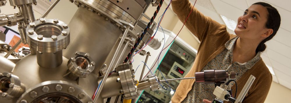
Reconstruction leads to two ‘types’ of C60 molecules on the surface, which exhibits differences in the covalent component of the substrate - adsorbate bond. (a) Clean Ni(110) Surface, (b) Quasi-Hexagonal 1 (QH1) Phase, (c) (5x3) Phase, (d) Carbide Adsorbate induced surface structures Adsorption on surfaces can lead to modifications of the surface structures. In many cases this manifests in minor modifications of the outermost atomic layers of the substrate, for example in changes to inter-layer spacings. In other cases however, the surface undergoes substantial reconstruction, causing significant changes in the atomic density of the outermost layers. In the case of metal on metal surfaces, surface alloying can also occur, representing a new class of materials. Our interest is in determining surface structures using a combination of LEED I-V analysis, STM and MEIS. The understanding of the growth of thin metallic films on metallic substrates has been the subject of much research over the last few years.
Whilst these systems are of interest from the viewpoint of technological applications, the growth processes can be complex, offering a range of interesting phenomenon at the atomic level. This is particularly the case for the growth of semi-metal overlayers, such as Pb, Sb and Bi on metal surfaces. Bismuth is a particularly attractive adsorbate material due to its small electron effective mass, anomalously high values of electron mean free path and mobility, highly anisotropic Fermi surface as well as having a long Fermi wavelength at room temperature, and small overlap between the conduction and valence bands. Furthermore, the growth of Bi nanowires by vapour deposition on Ag(111) was recently reported in an STM study. Such nanostructures are expected to exhibit interesting effects due to quantum confinement and finite size effects. The Bi-Ag(111) system is very similar to that of other metal on fcc(111) systems. Since Bi is immiscible with Ag, it is expected that the growth process would occur by formation of dense islands on the Ag(111) surface. However, like in other cases, it is found that at 1/3 ML coverage, a ,,- EMBED Equation.3 EMBED Equation.3 superstructure is observed as a result of surface alloy formation [6]. At higher coverage, above some critical value, a de-alloying process occurs and the monolayer growth leads to a dense plane above the Ag(111) surface.
The EMBED Equation.3 structure is of particular interest because the two dimensional alloy structure in both cases appears to behave like a 2-D electron gas with quantum confinement leading to spin-orbit coupling, known as the Rashba effect, which has implications for spintronics applications. Our results show that deposition of 1/3 of a monolayer of Bi on Ag(111) leads to the formation of BiAg2 surface alloy. A detailed analysis of this structure using LEED I-V measurements together with DFT calculations confirms that the Bi atom is found to replace one top layer Ag atom in each unit cell, forming a substitutional BiAg2 surface alloy.
Surface alloy structures
Pb, Sb and Bi on metal surfaces are particularly attractive adsorbate materials due to its small electron effective mass, anomalously high values of electron mean free path and mobility, highly anisotropic Fermi surface as well as having a long Fermi wavelength at room temperature, and small overlap between the conduction and valence bands. These semi-metal adsorbates on surfaces such as Ag(111) and Cu(111) are particularly interesting as they form a surface alloy that exhibits a strong spin-orbit coupling, leading to the so called Rashba effect.
Photovoltaic materials
The over dependence on fossil fuel for energy leading to global crisis in climate change has in recent years focused the political will to search for alternative sources of energy. The University of Liverpool has responded to this challenge by setting up a dedicated institute, the Stephenson Institute, investing in state-of-art equipment, research infrastructure and experts in several areas of research in renewable energy sources. The condensed matter physics group is part of this institute and is involved in experimental physics related to energy research and novel materials addressing the need to develop the next generation of semiconductor devices. One of the areas we have recently focused on is the interaction of Tellurium on copper surfaces. Copper is used as a back contact on CdTe thin film solar cell devices and the surface structure of this system is of current interest.
High-k materials
The continuous downscaling of devices to nanoscale dimensions, following Moore's law, means that silicon based complementary metal-oxide-semiconductor (CMOS) devices, which currently dominate the device industry, are reaching fundamental limits. Germanium is seen as a possible replacement for the Si pMOSFET channel material because of its high hole mobility and as a result there has been much interest in developing germanium based MOS technology. There are particular challenges for the Ge/high-permittivity (k) oxide stack which is now actively studied. Unlike Si, the native oxide of Ge is volatile and so an important issue in establishing Ge MOS technology is to develop a stable metal-insulator semiconductor (MIS) gate stack. To this end, attention has focused on GeO2/Ge interface control layer, which has the advantage of low interface state density and La2O3/Ge high-k oxide as an alternative.
Materials for fuel cells
Fuel cells provide for cleaner and more efficient conversion of fuel to energy via an electrochemical process. A fuel cell has an electrolyte that carries particles from one electrode to another and a catalyst that induces a reaction at the electrodes.
We are looking at the fundamental reactions that are involved at the electrode surfaces of materials such as platinum, copper and gold, and how they affect the electronic and geometrical structures of these surfaces.